Block Diagram Of 4 To 1 Multiplexer
A multiplexer schematic structure, b truth table of the mux based on Multiplexer 4x1 circuits mux multiplexers encoder inputs verilog code combinational udp theoretically 2n Multiplexer diagram block does work version quality
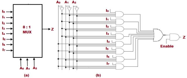
8 To 1 Multiplexer Logic Diagram And Truth Table | Elcho Table
Multiplexer diagram truth table digital javatpoint electronics block Mux multiplexer schematic structure inputs diagram considering Multiplexer digital electronics truth table diagram block javatpoint
Multiplekser demultiplexer multiplexer decoder implement encoder multiplexers precautions
Mux 3x1 diagram circuit4-to-1 multiplexer and demultiplexer 1 multiplexer design the pin diagram and functionMultiplexer in digital electronics.
Mux multiplexer cascading logic multiplexing bitsMultiplexer (mux) Block diagram and circuit diagram of 3x1 muxMultiplexer 4x1 applications diagram block advantages electricalvoice.
Multiplexer block diagram fpgas 4to1 figure
Mux multiplexer 8x1 diagram logic table truth schematic using input vlsi symbol 2x1 muxes diagrams figure structural structure elcho edaMy fpgas: modelling multiplexer Multiplexer demultiplexerMultiplexer in digital electronics.
Block diagram of 74150 -motorola cdm1250 wiring diagramMultiplexer diagram ic mux 8x1 table chegg function answered hasn expert ask question yet been Multiplexer combinational multiplexers multiplexores 16x1 multiplexor demultiplexer circuitos ciruitsDigital logic.

Multiplexer diagram block output verilog beginners figure
Block diagram of 4×1 multiplexerMultiplexer circuit precautions Verilog for beginners: 8-to-1 multiplexerCombinational logic ciruits-multiplexer and demultiplexer.
8 to 1 multiplexer logic diagram and truth table .


1 Multiplexer design The pin diagram and function | Chegg.com

My FPGAs: Modelling Multiplexer

Block Diagram Of 74150 -Motorola Cdm1250 Wiring Diagram | Begeboy

8 To 1 Multiplexer Logic Diagram And Truth Table | Elcho Table

Block diagram and circuit diagram of 3x1 MUX | Download Scientific Diagram

Block Diagram of 4×1 Multiplexer | Download Scientific Diagram

Multiplexer in Digital Electronics - Javatpoint

Multiplexer - Applications & Advantages | Electricalvoice

DeldSim - 4:1 Multiplexer Using IC 74LS153